Objective
The objective of this laboratory is to demonstrate the function of pull-up resistors.
Preparation
The following schematic details the hardware setup.
Table 1 lists the components used in the schematic.
| ID | Component | Manufacturer Part No. | Value | Qty. |
| Base Components | ||||
| IC1 | MCU | PIC24FJ256GA702-I/SP | – | 1 |
| IC2 | Regulator | LM1117T-3.3/NOPB | 3.3 V / 800 mA | 1 |
| C1 & C2 | Capacitor (tantalum) | TAP106K025SRW | 10 uF / 25 V | 2 |
| C3 & C4 | Capacitor (ceramic) | SR155C103KARTR1 | 0.01 uF / 50 V | 2 |
| C5 & C6 | Capacitor (ceramic) | SR155C104KARTR1 | 0.1 uF / 50 V | 2 |
| C7 & C8 | Capacitor (ceramic) | SR151A150JARTR1 | 15 pF / 100 V | 2 |
| C9 | Capacitor (ceramic) | FG16X7R1E106KRT06 | 10 uF / 25 V | 1 |
| Y1 | Crystal | ABL-16.000MHZ-B2 | 16 MHz | 1 |
| R1 | Resistor | SFR2500001002FR500 | 10 kΩ | 1 |
| R2 | Resistor | SFR2500001004FR500 | 1 MΩ | 1 |
| J1 | Header (6-way) (PICkit 5) | 22-27-2061 | – | 1 |
| Additional Components | ||||
| R3 | Resistor | SFR2500001400FR500 | 140 Ω | 1 |
| R4 | Resistor | SFR2500001002FR500 | 10 kΩ | 1 |
| D1 | LED (red) | WP132XID | 10 mA | 1 |
| SW1 | Switch (tactile) | FSM4JART | – | 1 |
Refer to the following source code.
/*                        Pull_Resistors (source code)                        */
/*                            MCU: PIC24FJ256GA702                            */
/*                              Author: Michael                               */

/**************************** Configuration Bits ******************************/

// FSEC
#pragma config BWRP = OFF                                                       // Boot Segment Write-Protect bit (Boot Segment may be written)
#pragma config BSS = DISABLED                                                   // Boot Segment Code-Protect Level bits (No Protection (other than BWRP))
#pragma config BSEN = OFF                                                       // Boot Segment Control bit (No Boot Segment)
#pragma config GWRP = OFF                                                       // General Segment Write-Protect bit (General Segment may be written)
#pragma config GSS = DISABLED                                                   // General Segment Code-Protect Level bits (No Protection (other than GWRP))
#pragma config CWRP = OFF                                                       // Configuration Segment Write-Protect bit (Configuration Segment may be written)
#pragma config CSS = DISABLED                                                   // Configuration Segment Code-Protect Level bits (No Protection (other than CWRP))
#pragma config AIVTDIS = OFF                                                    // Alternate Interrupt Vector Table bit (Disabled AIVT)

// FBSLIM
#pragma config BSLIM = 0x1FFF                                                   // Boot Segment Flash Page Address Limit bits (Enter Hexadecimal value)

// FOSCSEL
#pragma config FNOSC = PRIPLL                                                   // Oscillator Source Selection (Primary Oscillator with PLL module (XT + PLL, HS + PLL, EC + PLL))
#pragma config PLLMODE = PLL96DIV4                                              // PLL Mode Selection (96 MHz PLL. Oscillator input is divided by 4 (16 MHz input))
#pragma config IESO = OFF                                                       // Two-speed Oscillator Start-up Enable bit (Start up with user-selected oscillator source)

// FOSC
#pragma config POSCMD = HS                                                      // Primary Oscillator Mode Select bits (HS Crystal Oscillator Mode)
#pragma config OSCIOFCN = ON                                                    // OSC2 Pin Function bit (OSC2 is general purpose digital I/O pin)
#pragma config SOSCSEL = OFF                                                    // SOSC Power Selection Configuration bits (Digital (SCLKI) mode)
#pragma config PLLSS = PLL_PRI                                                  // PLL Secondary Selection Configuration bit (PLL is fed by the Primary oscillator)
#pragma config IOL1WAY = OFF                                                    // Peripheral pin select configuration bit (Allow multiple reconfigurations)
#pragma config FCKSM = CSDCMD                                                   // Clock Switching Mode bits (Both Clock switching and Fail-safe Clock Monitor are disabled)

// FWDT
#pragma config WDTPS = PS1                                                      // Watchdog Timer Postscaler bits (1:1)
#pragma config FWPSA = PR32                                                     // Watchdog Timer Prescaler bit (1:32)
#pragma config FWDTEN = OFF                                                     // Watchdog Timer Enable bits (WDT and SWDTEN disabled)
#pragma config WINDIS = OFF                                                     // Watchdog Timer Window Enable bit (Watchdog Timer in Non-Window mode)
#pragma config WDTWIN = WIN50                                                   // Watchdog Timer Window Select bits (WDT Window is 50% of WDT period)
#pragma config WDTCMX = WDTCLK                                                  // WDT MUX Source Select bits (WDT clock source is determined by the WDTCLK Configuration bits)
#pragma config WDTCLK = SYSCLK                                                  // WDT Clock Source Select bits (WDT uses system clock when active, LPRC while in Sleep mode)

// FPOR
#pragma config BOREN = OFF                                                      // Brown Out Enable bit (Brown Out Disabled)
#pragma config LPCFG = OFF                                                      // Low power regulator control (No Retention Sleep)
#pragma config DNVPEN = DISABLE                                                 // Downside Voltage Protection Enable bit (Downside protection disabled when BOR is inactive)

// FICD
#pragma config ICS = PGD1                                                       // ICD Communication Channel Select bits (Communicate on PGEC1 and PGED1)
#pragma config JTAGEN = OFF                                                     // JTAG Enable bit (JTAG is disabled)

// FDEVOPT1
#pragma config ALTCMPI = DISABLE                                                // Alternate Comparator Input Enable bit (C1INC, C2INC, and C3INC are on their standard pin locations)
#pragma config TMPRPIN = OFF                                                    // Tamper Pin Enable bit (TMPRN pin function is disabled)
#pragma config SOSCHP = ON                                                      // SOSC High Power Enable bit (valid only when SOSCSEL = 1 (Enable SOSC high power mode (default))
#pragma config ALTI2C1 = ALTI2CEN                                               // Alternate I2C pin Location (SDA1 and SCL1 on RB9 and RB8)

/************************* Configuration Bits (end) ***************************/

#define FCY 16000000                                                            // FCY = FOSC / 2 (FCY: Instruction clock cycle) (FOSC: System clock cycle)
#define LED_Red_1 LATBbits.LATB6                                                // LED_Red_1 associated with MCU Pin #15
#define Switch_1 PORTBbits.RB10                                                 // Switch_1 associaed with MCU Pin #21

#include <libpic30.h>                                                           // Delay functions
#include <xc.h>                                                                 // MCU pin mapping

int main(void)
{

    // Set pin direction
    TRISBbits.TRISB6 = 0;                                                       // MCU Pin #15 output (LED_Red_1)
    TRISBbits.TRISB10 = 1;                                                      // MCU Pin #21 input (Switch_1)

    /************************* configure MCU modules **************************/

    // Analog Ports
    ANSA = 0;                                                                   // Disable A (PIC24FJ256GA702 datasheet p.126 Table 11-1)
    ANSB = 0;

    // Comparators
    CM1CONbits.CEN = 0;                                                         // Disable #1 (PIC24FJ256GA702 datasheet p.310 Register 25-1)
    CM2CONbits.CEN = 0;
    CM3CONbits.CEN = 0;

    // ADC
    AD1CON1bits.ADON = 0;                                                       // Disable module (PIC24FJ256GA702 datasheet p.291 Register 24-1)

    /********************** configure MCU modules (end) ***********************/

    while (1)
    {

        if (Switch_1 == 0)                                                      // Switch_1 closed
        {
            LED_Red_1 = 1;                                                      // LED_Red_1 ON
        }

        else                                                                    // Switch_1 opened
        {
            LED_Red_1 = 0;                                                      // LED_Red_1 OFF
        }

    }

    return 0;

}Testing
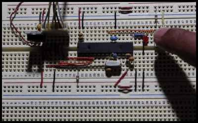
Press the button and observe the LED responding almost immediately by illuminating for a short period. Remove all components connected to pin #21 and then connect a wire to pin #21. Tap the exposed end of the wire with a finger and observe the LED illuminating randomly, indicating a floating point at pin #21.
Conclusion
The pull-up resistor, R4, eliminates the floating point at pin #21. The same concept applies to a pull-down resistor setup.