Transistors are commonly used for one of two purposes, i.e., switching or amplification. There are numerous electronic chips, such as MCUs, OLED displays, and sensors, which generally utilise one of two transistor architectures, i.e., Transistor-Transistor Logic (TTL) or Complimentary Metal Oxide Semiconductor (CMOS), as shown in Table 1.
| Type | Symbol | |||
| BJTs | NPN | 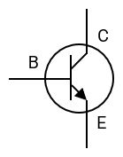 | ||
| PNP | 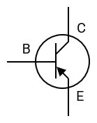 | |||
| FETs | MOSFETs | Enhancement | N-Channel |   |
| P-Channel |  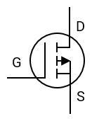 | |||
| Depletion | N-Channel |  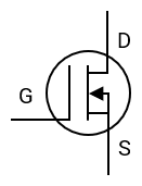 | ||
| P-Channel |   | |||
| JFETs | Depletion | N-Channel |  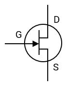 | |
| P-Channel |  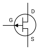 | |||
Bipolar Junction Transistors (BJTs) fall under the umbrella of TTL, which is a combination of BJTs to achieve a specific result, such as a full-wave amplifier. Chips that utilise TTL architecture typically use the Voltage Common Collector (VCC) naming convention to indicate the power input. A BJT can also be used on its own, either a NPN or PNP type, to achieve a specific result.
Field Effect Transistors (FETs) fall under the umbrella of CMOS, which is a combination of FETs to achieve a specific result, such as driving a motor in both directions. Chips that utilise CMOS architecture typically use the Voltage at Drain (VDD) naming convention to indicate the power input. A FET can also be used on its own, either an Enhancement or Depletion type, to achieve a specific result.
Table 2 lists the major differences between BJTs and MOSFETs.
| Characteristic | BJT | MOSFET |
| Technology | Old | New |
| Application | Low-Current | High-Current |
| Switching Speed | Slow | Fast |
| Power Consumption | High | Low |
| Control Method | Current | Voltage |
| Input Impedance | Low | High |
| Heat Dissipation | High | Low |
| Charge Carriers | Bi-Polar | Unipolar |
| Footprint | Large | Small |
| Cost | Cheap | Expensive |
The main strength of BJTs is that they are suitable for low-current applications, such as amplifying analog signals. The main strength of MOSFETs is that they are suitable for high-current applications, such as driving a motor. A BJT is a current-controlled current device, meaning that an input current controls an output current. A FET is a voltage-controlled current device, meaning that an input voltage controls an output current. This page focuses on BJTs and MOSFETs (Enhancement), since these transistors are more common.
BJT (NPN)
There are three terminals in a BJT NPN: Base (B), Collector (C), and Emitter (E), as shown in Figure 1.
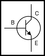
A signal with a small current is applied to the Base, to control a larger current from the Collector to the Emitter. Note that the word current (I) is used to indicate the flow of conventional current, i.e., from a higher potential (+) to a lower potential (-). This is in opposition to the flow of electrons, i.e., from a lower potential (-) to a higher potential (+).
Table 3 outlines the three operating modes for a NPN transistor.
| Mode | Voltages | Schematic |
| Cut-Off | VC > VB VE > VB VB << VBE(sat) | 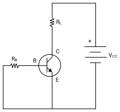 |
| A NPN running in Cut-Off mode is essentially an “open-switch”, in which there is no current flowing through the Collector. This is because the Base voltage (VB) is lower than the Collector and Emitter voltages, VC and VE, respectively, and well below the saturation voltage (VBE(sat)). The saturation voltage, found in the manufacturer data sheet, is the minimum voltage applied to the Base, at which there is a maximum flow of current through the Collector, i.e., VCC / RL. Note that all terminal voltages are relative to the Emitter. If a motor is connected as the load, the motor’s shaft will not rotate at all. | ||
| Active | VC > VB > VE VB < VBE(sat) | 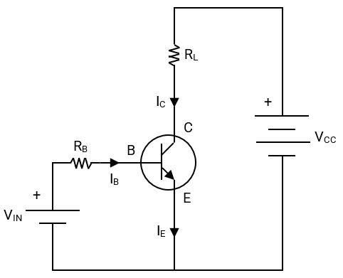  |
| A NPN running in Active mode is essentially an amplifier, in which there is some current flowing through the Collector. This is because the Base voltage is lower than the Collector voltage, higher than the Emitter voltage, and below the saturation voltage. As the Base voltage increases, the voltage at the Collector decreases, thereby increasing the Collector current. If a motor is connected as the load, the motor’s shaft will rotate at a fraction of the motor’s full speed. | ||
| Saturation | VC < VB VE < VB VB ≥ VBE(sat) | 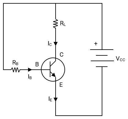 |
| A NPN running in Saturation mode is essentially a “closed-switch”, in which there is full current flowing through the Collector. This is because the Base voltage is higher than the Collector and Emitter voltages and higher than or equal to the saturation voltage. At this point, increasing the Base voltage does not increase the Collector current. If a motor is connected as the load, the motor’s shaft will rotate at full speed. | ||
As can be seen, a NPN transistor is used for low-side switching. The load is connected to the Collector, in most cases, because if the load is connected to the Emitter, the current flowing through the load (IE) will be the sum of the Base and Collector currents, IB and IC, respectively, which is not easy to control since the Base current is not easy to control. In other words, the Collector current is stable. Note that some BJTs are capable of both switching and amplification, while other BJTs are designed for switching or amplification only.
Figure 2 represents a breakdown of the BJT NPN operating in Active mode.
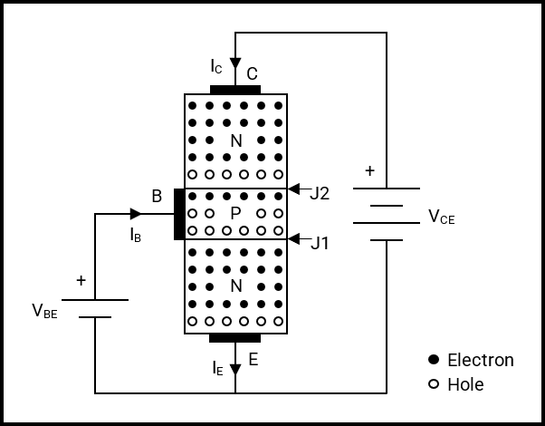
There are two N-type materials that “sandwich” a P-type material. A N-type material contains a majority of free electrons (black dots), negative charge carriers, and a minority of holes (black circles), positive charge carriers. A P-type material contains a minority of free electrons and a majority of holes. Compared to the Collector and Emitter, the Base material is much thinner, hence containing far fewer electrons and holes.
A small voltage, VBE, is applied between the Base and Emitter, making the P-N junction, J1, forward-bias. In other words, “P” and “N” are connected to the positive and negative terminals, respectively, of the voltage source (VBE). With J1 in forward-bias, electrons migrate from the negative (-) terminal of the voltage source, enter the Emitter, and migrate towards the base, crossing over J1, where the minority of them combine with holes. Whilst one electron is combining with a hole, in the Base, another electron, in the Base, is uncombining from a hole and migrating towards the positive (+) terminal of the voltage source, creating the Base current.
A larger voltage, VCB, than VBE, is applied between the Collector (N) and Base, making the P-N junction, J2, reverse-biased. In other words, “P” is connected to the positive terminal of the voltage source (VBE), while “N” is connected to the positive terminal of the voltage source (VCE). With J2 in reverse-bias, the majority of electrons migrating towards the base, from the Emitter, migrate towards the Collector, crossing over J2, where they migrate towards the (+) terminal of the power source (VCE), creating the Collector current.
Applying Kirchhoff’s Voltage Law (KVL) to the transistor in Figure 2 reveals the relationships between the Emitter, Base, and Collector voltages, as shown in Equation 1. Applying Kirchhoff’s Current Law (KCL) to the transistor in Figure 2 reveals the relationship between the Emitter, Base, and Collector currents, as shown in Equation 2. The Base current carries the minority of total current flow, where a small change to the Base current results in a large change to the Collector current, i.e. a current gain (β), as shown in Equation 3.
\begin{equation}
\tag{1}
\mathrm{V_{CE} = V_{CB} + V_{BE}}
\end{equation}
\begin{equation}
\tag{2}
\mathrm{I_{E} = I_{B} + I_{C}}
\end{equation}
\begin{equation}
\tag{3}
\mathrm{β= \frac{I_{C}} {I_{B}}}
\end{equation}
The PNP transistor is identical to the NPN transistor except the voltages and currents are reversed. Table 4 lists the main differences between a NPN and PNP BJT.
| Characteristic | NPN | PNP |
| Utilisation | High | Low |
| Switching (typical) | Low-Side | High-Side |
| Charge Carriers (majority) | Electrons | Holes |
| Charge Carriers (minority) | Holes | Electrons |
| Current (capacity) | High | Low |
| Switching Speed | Fast | Slow |
| Base Voltage (LOW) | OFF | ON |
| Base Voltage (HIGH) | ON | OFF |
| Saturation | VB > VC VB > VE | VB < VC VB < VE |
| Active | VC > VB > VE | VC < VB < VE |
| Cut-Off | VB < VC VB < VE | VB > VC VB > VE |
NPN transistors are utilised more than PNP transistors due to their higher electron mobility, i.e., ability to handle higher currents and faster switching speeds. If the voltage applied to the Base of a NPN transistor is LOW, the transistor switches OFF, and switches ON if the voltage applied to the Base is HIGH. If the voltage applied to the Base of a PNP transistor is HIGH, the transistor switches OFF, and switches ON if the voltage applied to the Base is LOW.
MOSFET Enhancement (N-Channel)
There are three terminals in a MOSFET Enhancement N-Channel: Gate (G), Drain (D), and Source (S), as shown in Figure 3.
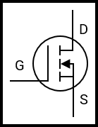
A signal, with a small voltage, is applied to the Gate to control a current from the Drain to the Source.
Table 5 outlines the three operating modes of the N-Channel transistor.
| Mode | Voltages | Schematic |
| Cut-Off | VGS < VGS(th) | 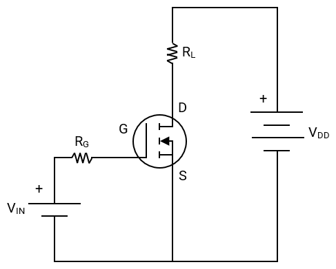 |
| A N-Channel transistor running in Cut-Off mode is essentially an “open-switch”, in which there is no, or an extremely small leakage, Drain-to-Source current (IDS) flowing. This is because the Gate-to-Source voltage (VGS) is lower than the Gate-to-Source threshold voltage (VGS(th)). The Gate-to-Source threshold voltage, which can be found in the manufacturer data sheet, is the minimum voltage applied between the Gate and Source terminals, at which there is a conductive channel established between the Drain and Source terminals. If a motor is connected as the load, the motor’s shaft will not rotate at all. | ||
| Saturation | VGS > VGS(th) VDS > VDS(sat) or VDS > VGS – VGS(th) | 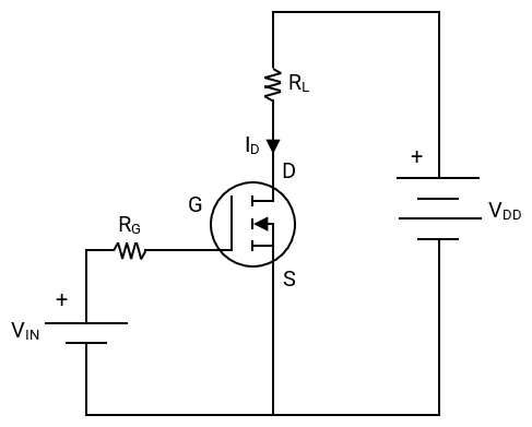  |
| A N-Channel transistor running in Saturation mode is essentially an amplifier, in which there is a fraction of the full Drain-to-Source current flowing. This is because the Gate-to-Source voltage is higher than the Gate-to-Source threshold voltage, and the Drain-to-Source voltage (VDS) is higher than the Drain-to-Source saturation voltage (VDS(sat)). If a motor is connected as the load, the motor’s shaft will rotate at a fraction of the motor’s full speed. | ||
| Linear | VGS > VGS(th) VDS < VDS(sat) or VDS < VGS – VGS(th) | 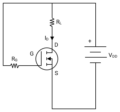 |
| A N-Channel transistor running in Linear mode is essentially a “closed-switch”, in which there is full Drain-to-Source current flowing. This is because the Gate-to-Source voltage is higher than the Gate-to-Source threshold voltage, and the Drain-to-Source voltage is lower than the Drain-to-Source saturation voltage. If a motor is connected as the load, the motor’s shaft will rotate at the motor’s full speed. | ||
As can be seen, a N-Channel transistor is used for low-side switching. Note that all MOSFETs are not capable of both switching and amplification, i.e., some MOSFETs are specifically designed for switching, while others are specifically designed for amplification.
Figure 4 represents a breakdown of the N-Channel transistor operating in the Cut-Off mode.
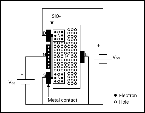
There are two N-type materials embedded within the P-type substrate, to which the Drain and Source terminals are connected. A silicon dioxide (SiO2) layer is “sandwiched” in between the Gate terminal and P-type substrate, creating an insulation barrier. Note that the Body (B) terminal connects the P-type substrate to the N-type material via the Source terminal in most MOSFETs. Until the voltage applied between the Gate and Source terminals is more than the Gate-to-Source threshold voltage, no current will flow from the Drain to Source terminals since there is no conductive channel established in between the Drain and Source terminals.
Figure 5 represents a breakdown of the N-Channel transistor operating in Saturation mode.
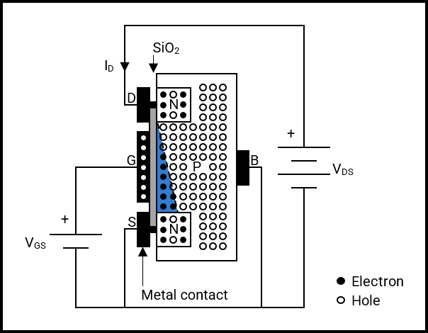
A small voltage, VGS, is applied between the Gate and Source terminals, where the metal contact at the Gate terminal accumulates a positive charge, i.e., holes. The positively charged contact causes free electrons within the N-type material, at the Source terminal, to migrate towards the P-type substrate, filling holes in between the Source and Drain terminals and accumulating adjacent to the silicon dioxide layer. The silicon dioxide layer, separating the positively charged contact from the accumulated electrons, mimics the dielectric material in a capacitor, meaning that no accumulated electrons can reach the contact. This makes the input impedance in a MOSFET very high, leading to the term “Field Effect”.
If the voltage between the Gate and Source terminals is just below the Gate-to-Source threshold voltage, a scenario called the “pinch-off” point is reached, in which a triangular-shaped region exists in between the Drain and Source terminals, as shown in Figure 6.
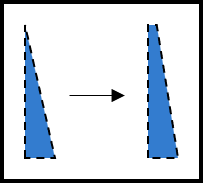
This may appear to be a conductive path in between these terminals; however, the pointed end towards the Drain terminal is infinitesimally small. If the voltage between the Gate and Source terminals is at the Gate-to-Source threshold voltage, a conductive channel is established in between the Drain and Source terminals, represented by the trapezoidal shape. Increasing the voltage between the Gate and Source terminals results in more free electrons accumulating adjacent to the silicon dioxide barrier, which in turn widens, i.e., enhances the channel. With an enhanced channel, a greater current can flow the Drain to Source terminals.
A larger voltage, VDS, compared to VGS, is applied between the Drain and Source terminals, where electrons leave the negative (-) terminal, migrate through the N-Type material in the Source terminal, migrate through the established channel, migrate through the N-Type material in the Drain terminal, and finally migrate towards the positive (+) terminal of the power source.
Figure 7 represents a breakdown of the N-Channel transistor operating in the Linear mode.
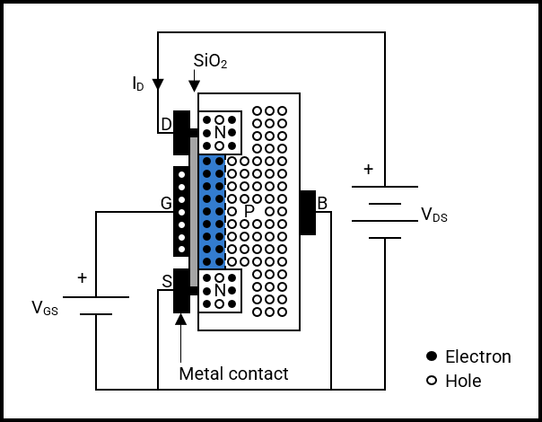
If the voltage in between the Gate and Source terminals reaches a certain value, i.e., well above the threshold voltage, the original triangular conductive path now becomes rectangular, which implies a maximum flow of current from the Drain terminal to the Source terminal. In other words, increasing VGS will not further increase the flow of current from the Drain terminal to the Source terminal.
The MOSFET Enhanced P-Channel is identical to the MOSFET Enhanced N-Channel; however, everything is reversed, i.e., currents and voltages.