Objective
The objective of this laboratory is to establish an MCU platform for further laboratories and projects by controlling an LED.
Preparation
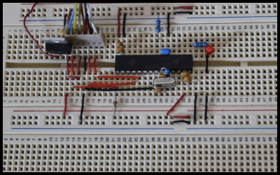
The following schematic details the hardware setup. Click on the +, -, and >> icons to zoom into, zoom out of, and pan the image with the hand tool, respectively.
Table 1 lists the components used in the schematic. The first eleven components are the base components for the MCU and the remaining two additional components are directly related to this laboratory. Electronic component wholesalers may be out of stock for certain components; hence, an alternative must be found. Note that it is not necessary to use identical components, as long as similar characteristics are used. Note that the majority of components for laboratory exercises presented on this website are best used with a breadboard to make the circuit design and testing process streamlined.
| ID | Component | Manufacturer Part No. | Value | Qty. |
| Base Components | ||||
| IC1 | MCU | PIC24FJ256GA702-I/SP | – | 1 |
| IC2 | Regulator | LM1117T-3.3/NOPB | 3.3 V / 800 mA | 1 |
| C1 & C2 | Capacitor (tantalum) | TAP106K025SRW | 10 uF / 25 V | 2 |
| C3 & C4 | Capacitor (ceramic) | SR155C103KARTR1 | 0.01 uF / 50 V | 2 |
| C5 & C6 | Capacitor (ceramic) | SR155C104KARTR1 | 0.1 uF / 50 V | 2 |
| C7 & C8 | Capacitor (ceramic) | SR151A150JARTR1 | 15 pF / 100 V | 2 |
| C9 | Capacitor (ceramic) | FG16X7R1E106KRT06 | 10 uF / 25 V | 1 |
| Y1 | Crystal | ABL-16.000MHZ-B2 | 16 MHz | 1 |
| R1 | Resistor | SFR2500001002FR500 | 10 kΩ | 1 |
| R2 | Resistor | SFR2500001004FR500 | 1 MΩ | 1 |
| J1 | Header (6-way) (PICkit 5) | 22-27-2061 | – | 1 |
| Additional Components | ||||
| R3 | Resistor | SFR2500001400FR500 | 140 Ω | 1 |
| D1 | LED (red) | WP132XID | 10 mA | 1 |
Table 2 is a list of instructions to setup the hardware.
| STEP | Description |
| 1 | Download the datasheet for the PIC24FJ256GA702 MCU. |
| 2 | Briefly read through the first page, paying close attention to the operating voltage range (2 V to 3.6 V), register size (16-bit), and maximum system clock frequency (FOSC = 32 MHz). |
| 3 | The power supply includes a voltage regulator (LM1117T-3.3/NOPB) (3.3 V). As per the datasheet, a decoupling/bypass tantalum capacitor of 10 µF is required on both the input and output of the regulator. Note that this particular regulator is fixed, as shown in Figure 9-3 on page 16 of the datasheet. These capacitors filter out electrical noise in addition to acting like a temporary “backup battery” in the event of a momentary voltage drop. |
| 4 | Page 4 details the pin layout for the DIP package. There are two VDD power supply pins, i.e., pin #13 and pin #28, and three Vss ground/reference pins, i.e., pin #8, pin #19, and pin #27. All these pins must be connected accordingly. Decoupling capacitors are placed on both VDD pins and the VCAP pin. Pin #1, Master Clear Reset (MCLR), serves two purposes: for programming and resetting the MCU. The 10 kΩ resistor between the MCLR pin and the 3.3 V power rail prevents higher voltages that are applied to the MCLR pin during programming from reaching the 3.3 V power rail. The same resistor is also a pull-up resistor, preventing the MCU from randomly resetting in the case of having no such resistor. Pins #4 & #5 serve for programming via the programming tool’s data and clock lines, respectively. The programming tool used in this laboratory is the PICkit 5 by Microchip. Other programming tools can be used. Ensure that the pins of the programming tool are connected to the MCU correctly, via the J1 header. Pins RA0 to RA4 and RB0 to RB15 are all Input/Output (I/O) pins, meaning that they can transmit or receive data. Pins marked with RPn can be mapped to certain modules of the MCU, such as the Universal Asynchronous Transmitter Receiver (UART), Analog to Digital Converters (A/D), timers, etc. |
| 5 | The crystal oscillator, across Pins #9 & #10, sets the timing for the MCU. As per the dsPIC33/PIC24 Family Reference Manual Oscillator Module datasheet, two capacitors on both pins of the ABL-16.000MHZ-B2 crystal and a 1 MΩ parallel resistor across the crystal are required for stability. |
| 6 | An LED, in series with a 140 Ω resistor, is connected to pin #15 of the MCU. The calculation of the resistor value uses Ohm’s Law, as shown in Eqn 1. Note that the current through the LED operating at 1.9 V is 10 mA. |
\begin{equation}
\tag{1}
V = IR
\end{equation}
\begin{equation}
\tag{2}
V_{Pin15} = 0.01R+V_{LED}
\end{equation}
\begin{equation}
\tag{3}
3.3 = 0.01R+1.9
\end{equation}
\begin{equation}
\tag{4}
R = 140 \,\Omega
\end{equation}
Download and install the MPLAB X Integrated Development Environment (IDE) and the 16-bit compiler, MPLAB XC16, from the Microchip website. Video 1 demonstrates how to set up the Microchip MPLAB X IDE for developing embedded software. Set the video to full-screen to get a better resolution. Note there is no sound in this video.
Table 3 lists various timestamps with a description.
| Timestamp | Description |
| Preparation | Connect the PICkit 5 to a computer the PIC24FJ256GA702. |
| 0:22 | Select PICkit 5 under the “Tool:” dropdown menu. Note that at the time of making this video, the ICD 3 tool was used with MPLAB X IDE v6.00, which is now unsupported with versions of MPLAB X IDE from v6.25 onwards. |
| 0:45 | The main file for an embedded system is called the source file with the “.c” file extension. |
| 0:57 | The auxiliary file for an embedded system is called the header file with the “.h” file extension. Header files, as demonstrated in the MPLAB Libraries page, are used for software libraries that can be called upon within the source file. For this laboratory, custom header files are not used. |
| 1:02 | Set the Configuration Bits, following the code below (lines #8 to #55), and click the “Generate Source Code to Output” button to result in a list of configuration bits just like the code below. The configuration bits govern the behaviour of the MCU. |
The following source code can be copied and pasted into MPLAB X IDE; however, it is a good learning experience to get used to typing code. Pay attention to the comments, which describe the lines of code.
/*                             MCUs (source code)                             */
/*                            MCU: PIC24FJ256GA702                            */
/*                              Author: Michael                               */

/**************************** Configuration Bits ******************************/

// FSEC
#pragma config BWRP = OFF                                                       // Boot Segment Write-Protect bit (Boot Segment may be written)
#pragma config BSS = DISABLED                                                   // Boot Segment Code-Protect Level bits (No Protection (other than BWRP))
#pragma config BSEN = OFF                                                       // Boot Segment Control bit (No Boot Segment)
#pragma config GWRP = OFF                                                       // General Segment Write-Protect bit (General Segment may be written)
#pragma config GSS = DISABLED                                                   // General Segment Code-Protect Level bits (No Protection (other than GWRP))
#pragma config CWRP = OFF                                                       // Configuration Segment Write-Protect bit (Configuration Segment may be written)
#pragma config CSS = DISABLED                                                   // Configuration Segment Code-Protect Level bits (No Protection (other than CWRP))
#pragma config AIVTDIS = OFF                                                    // Alternate Interrupt Vector Table bit (Disabled AIVT)

// FBSLIM
#pragma config BSLIM = 0x1FFF                                                   // Boot Segment Flash Page Address Limit bits (Enter Hexadecimal value)

// FOSCSEL
#pragma config FNOSC = PRIPLL                                                   // Oscillator Source Selection (Primary Oscillator with PLL module (XT + PLL, HS + PLL, EC + PLL))
#pragma config PLLMODE = PLL96DIV4                                              // PLL Mode Selection (96 MHz PLL. Oscillator input is divided by 4 (16 MHz input))
#pragma config IESO = OFF                                                       // Two-speed Oscillator Start-up Enable bit (Start up with user-selected oscillator source)

// FOSC
#pragma config POSCMD = HS                                                      // Primary Oscillator Mode Select bits (HS Crystal Oscillator Mode)
#pragma config OSCIOFCN = ON                                                    // OSC2 Pin Function bit (OSC2 is general purpose digital I/O pin)
#pragma config SOSCSEL = OFF                                                    // SOSC Power Selection Configuration bits (Digital (SCLKI) mode)
#pragma config PLLSS = PLL_PRI                                                  // PLL Secondary Selection Configuration bit (PLL is fed by the Primary oscillator)
#pragma config IOL1WAY = OFF                                                    // Peripheral pin select configuration bit (Allow multiple reconfigurations)
#pragma config FCKSM = CSDCMD                                                   // Clock Switching Mode bits (Both Clock switching and Fail-safe Clock Monitor are disabled)

// FWDT
#pragma config WDTPS = PS1                                                      // Watchdog Timer Postscaler bits (1:1)
#pragma config FWPSA = PR32                                                     // Watchdog Timer Prescaler bit (1:32)
#pragma config FWDTEN = OFF                                                     // Watchdog Timer Enable bits (WDT and SWDTEN disabled)
#pragma config WINDIS = OFF                                                     // Watchdog Timer Window Enable bit (Watchdog Timer in Non-Window mode)
#pragma config WDTWIN = WIN50                                                   // Watchdog Timer Window Select bits (WDT Window is 50% of WDT period)
#pragma config WDTCMX = WDTCLK                                                  // WDT MUX Source Select bits (WDT clock source is determined by the WDTCLK Configuration bits)
#pragma config WDTCLK = SYSCLK                                                  // WDT Clock Source Select bits (WDT uses system clock when active, LPRC while in Sleep mode)

// FPOR
#pragma config BOREN = OFF                                                      // Brown Out Enable bit (Brown Out Disabled)
#pragma config LPCFG = OFF                                                      // Low power regulator control (No Retention Sleep)
#pragma config DNVPEN = DISABLE                                                 // Downside Voltage Protection Enable bit (Downside protection disabled when BOR is inactive)

// FICD
#pragma config ICS = PGD1                                                       // ICD Communication Channel Select bits (Communicate on PGEC1 and PGED1)
#pragma config JTAGEN = OFF                                                     // JTAG Enable bit (JTAG is disabled)

// FDEVOPT1
#pragma config ALTCMPI = DISABLE                                                // Alternate Comparator Input Enable bit (C1INC, C2INC, and C3INC are on their standard pin locations)
#pragma config TMPRPIN = OFF                                                    // Tamper Pin Enable bit (TMPRN pin function is disabled)
#pragma config SOSCHP = ON                                                      // SOSC High Power Enable bit (valid only when SOSCSEL = 1 (Enable SOSC high power mode (default))
#pragma config ALTI2C1 = ALTI2CEN                                               // Alternate I2C pin Location (SDA1 and SCL1 on RB9 and RB8)

/************************* Configuration Bits (end) ***************************/

#define FCY 16000000                                                            // FCY = FOSC / 2 (FCY: Instruction clock cycle) (FOSC: System clock cycle)
#define LED_Red_1 LATBbits.LATB6                                                // LED_Red_1 associated with MCU Pin #15

#include <libpic30.h>                                                           // Delay functions
#include <xc.h>                                                                 // MCU pin mapping

int main(void)
{

    // Set pin direction
    TRISBbits.TRISB6 = 0;                                                       // MCU Pin #15 output (LED_Red_1)

    /************************* configure MCU modules **************************/

    // Analog Ports
    ANSA = 0;                                                                   // Disable A (PIC24FJ256GA702 datasheet p.126 Table 11-1)
    ANSB = 0;

    // Comparators
    CM1CONbits.CEN = 0;                                                         // Disable #1 (PIC24FJ256GA702 datasheet p.310 Register 25-1)
    CM2CONbits.CEN = 0;
    CM3CONbits.CEN = 0;

    // ADC
    AD1CON1bits.ADON = 0;                                                       // Disable module (PIC24FJ256GA702 datasheet p.291 Register 24-1)

    /********************** configure MCU modules (end) ***********************/

    while (1)
    {
        LED_Red_1 = 1;                                                          // LED_Red_1 ON
        __delay_ms(1000);                                                       // Delay (1000ms)
        LED_Red_1 = 0;                                                          // LED_Red_1 OFF
        __delay_ms(1000);
    }

    return 0;

}Testing
Video 2 demonstrates how to use the Microchip MPLAB X IDE for programming the source code onto the MCU.
After pressing the “Make and Program Device Main Project” button, the bottom-half window will display a script detailing the progress of the programming procedure. If an error comes up such as “Failed to get Device ID. Please make sure the target device is attached and try the operation again”. Please see the following Microchip help page.
If the programming procedure is successful, a “Programming/Verify complete” message will appear at the bottom. Observe the LED flashing ON and OFF for 1-second intervals, indicating the timing of the MCU is functioning as expected as a first-pass test, as shown in the picture at the beginning of this page. The delay can be increased to 10,000 ms for further testing. Further measurements are required, with an oscilloscope, to confirm the crystal is functioning with precision. Figures 1 & 2 represent an oscilloscope measurement of the crystal oscillator, probed at Pin #10 (CLKO), of the MCU.

In total, there are a total of three intervals, i.e., TOSCD, TOST, and TLOCK. TOSCD is the interval before the crystal oscillator oscillates below and above the VIL(max) and VIH(min) thresholds, respectively. The intersection between the vertical dotted line and the VIL(max) and VIH(min) lines marks the point when the crystal oscillator starts oscillating within acceptable logic levels.

Following the TOSCD interval, the Oscillator Startup Timer (TOST) has a 10-bit counter that counts 1024 crystal oscillator cycles, i.e., 64 μs. Following the TOST interval, there is an additional delay of 24 μs for the Phase Lock Loop (PLL) to lock, TLOCK, before a stable crystal oscillator signal can be released to the rest of the system. Note that every time the crystal oscillator starts/restarts, these three intervals are repeated.
Figure 3 represents the frequency counter counting 16.0002 MHz on the crystal’s signal.

Crystal manufacturers specify a load capacitance (CL) which is the required capacitance that must be applied in parallel to the crystal to achieve its set frequency, i.e., in this case it is 16 MHz. Equations 5 & 6 demonstrate how to calculate the capacitor value for external capacitors C7 & C8, which are used to fine-tune the crystal’s operating frequency.
\begin{equation}
\tag{5}
C_{L} = C_{S} + \frac{C_{7} \cdot C_{8}}{C_{7} + C_{8}}
\end{equation}
\begin{equation}
\tag{6}
C_{7} = C_{8} = 2(C_{L} – C_{S}) = 2(18 – 10.5) = 15 \,pF
\end{equation}
The load capacitance for the crystal, as per the manufacturer’s datasheet, is 18 pF. Capacitance, Cs, represents the stray capacitance around the terminals of the crystal, in addition to that found within the traces of a PCB and around neighbouring MCU pins. Determining the value of Cs is not straightforward but is usually within the range from 2 pF to 5 pF of a well-designed PCB layout. In this case; however, a breadboard is used, which results in a significantly higher stray capacitance of approximately 10.5 pF. This value was found by a matter of trial and error by using the frequency counter on an oscilloscope to get as close as possible to 16 MHz, with a variety of capacitors in the range of 10 pF up to 27 pF. A pair of capacitors with a value of 15 pF was found to result in a frequency count of 16,000,200 Hz, which is fairly close to the ideal operating frequency of 16,000,000 Hz.
The drift, i.e., error, is calculated as demonstrated in Equation 7.
\begin{equation}
\tag{7}
t_{Drift}= (\frac{ f }{{f_{o}}} -1) \cdot Duration = (\frac{ 16,000,200 }{{16,000,000}} -1) \cdot 8,760 = 0.1095 \,hrs/year
\end{equation}
For a drift of 0.1095 hrs per year, i.e., 394.2 s, this is generally acceptable. Depending on the application, using a well-designed PCB layout is crucial to reducing crystal drift. Using larger-value capacitors results in a greater negative drift from the desired frequency, i.e., <16 MHz. Using smaller value capacitors results in a greater positive drift from the desired frequency, i.e., >16 MHz.
Conclusion
Based on measurements and the behaviour of the LED, the MCU is functioning as expected and can therefore be used as the basis of projects.