| Note that this laboratory uses the APC220 radio module, which has an operating frequency range from 418MHz to 455MHz, and a maximum power output of 20mW. The laws pertaining to the operation of radio equipment must be adhered to and vary from country to country. |
Objective
The objective of this laboratory is to send specific messages from a computer serial terminal to an MCU such that the MCU will illuminate a green or yellow LED and illuminate a red LED if there is an overrun error.
Preparation
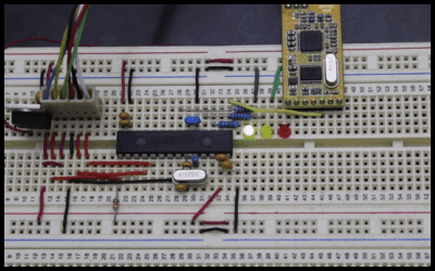
The following schematic details the hardware setup.
Note that the MCU Pin #15 is 5 V tolerant, so it can accept 5 V signals from the APC220. Table 1 lists the components used in the schematic.
| ID | Component | Manufacturer Part No. | Value | Qty. |
| Base Components | ||||
| IC1 | MCU | PIC24FJ256GA702-I/SP | – | 1 |
| IC2 | Regulator | LM1117T-3.3/NOPB | 3.3 V / 800 mA | 1 |
| C1 & C2 | Capacitor (tantalum) | TAP106K025SRW | 10 uF / 25 V | 2 |
| C3 & C4 | Capacitor (ceramic) | SR155C103KARTR1 | 0.01 uF / 50 V | 2 |
| C5 & C6 | Capacitor (ceramic) | SR155C104KARTR1 | 0.1 uF / 50 V | 2 |
| C7 & C8 | Capacitor (ceramic) | SR151A150JARTR1 | 15 pF / 100 V | 2 |
| C9 | Capacitor (ceramic) | FG16X7R1E106KRT06 | 10 uF / 25 V | 1 |
| Y1 | Crystal | ABL-16.000MHZ-B2 | 16 MHz | 1 |
| R1 | Resistor | SFR2500001002FR500 | 10 kΩ | 1 |
| R2 | Resistor | SFR2500001004FR500 | 1 MΩ | 1 |
| J1 | Header (6-way) (PICkit 5) | 22-27-2061 | – | 1 |
| Additional Components | ||||
| IC3 | Radio module | APC220 | – | 1 |
| IC4 | Regulator | LM1086IT-5.0/NOPB | 5 V / 1.5 A | 1 |
| C10 & C11 | Capacitor (tantalum) | TAP106K025SRW | 10 uF / 25 V | 2 |
| R3 – R5 | Resistor | SFR2500001400FR500 | 140 Ω | 1 |
| D1 | LED (green) | WP132XGD | 10 mA | 1 |
| D2 | LED (yellow) | WP132XYD | 10 mA | 1 |
| D3 | LED (red) | WP132XID | 10 mA | 1 |
The APC220 radio module requires a USB adapter and software, RF-Magic, to be installed for setting operating characteristics. Note that the APC220 module must be connected to a computer via a USB adapter before launching the APC220 software. Run the software as an administrator, as shown in Figure 1.

Upon opening the software, a message at the bottom should appear, “Found device!”, indicating that the APC220 module is ready to be configured. As per the datasheet, the APC220 operates within the range of 418 MHz to 455 MHz. A frequency can be chosen and entered into the RF frequency field. Select an RF TRx rate of 9600 bps, which is common. The NET ID and NODE ID can be set as desired. The Series Parity is disabled. The PC Series indicates the COM port that the APC220 is using. Press the Write ‘W’ button to program the APC220 module. A “write succeed!” message should be displayed at the bottom of the window. The Read R button can be pressed to confirm that the APC220 module is programmed as intended. Similarly, a “read succeed!!” message should be displayed at the bottom of the window. Note that subsequent APC220 modules, to be programmed, must all share the exact same parameters, except for the NODE ID, which must be unique.
Refer to the following source code.
/*                             UART (source code)                             */
/*                            MCU: PIC24FJ256GA702                            */
/*                              Author: Michael                               */

/**************************** Configuration Bits ******************************/

// FSEC
#pragma config BWRP = OFF                                                       // Boot Segment Write-Protect bit (Boot Segment may be written)
#pragma config BSS = DISABLED                                                   // Boot Segment Code-Protect Level bits (No Protection (other than BWRP))
#pragma config BSEN = OFF                                                       // Boot Segment Control bit (No Boot Segment)
#pragma config GWRP = OFF                                                       // General Segment Write-Protect bit (General Segment may be written)
#pragma config GSS = DISABLED                                                   // General Segment Code-Protect Level bits (No Protection (other than GWRP))
#pragma config CWRP = OFF                                                       // Configuration Segment Write-Protect bit (Configuration Segment may be written)
#pragma config CSS = DISABLED                                                   // Configuration Segment Code-Protect Level bits (No Protection (other than CWRP))
#pragma config AIVTDIS = OFF                                                    // Alternate Interrupt Vector Table bit (Disabled AIVT)

// FBSLIM
#pragma config BSLIM = 0x1FFF                                                   // Boot Segment Flash Page Address Limit bits (Enter Hexadecimal value)

// FOSCSEL
#pragma config FNOSC = PRIPLL                                                   // Oscillator Source Selection (Primary Oscillator with PLL module (XT + PLL, HS + PLL, EC + PLL))
#pragma config PLLMODE = PLL96DIV4                                              // PLL Mode Selection (96 MHz PLL. Oscillator input is divided by 4 (16 MHz input))
#pragma config IESO = OFF                                                       // Two-speed Oscillator Start-up Enable bit (Start up with user-selected oscillator source)

// FOSC
#pragma config POSCMD = HS                                                      // Primary Oscillator Mode Select bits (HS Crystal Oscillator Mode)
#pragma config OSCIOFCN = ON                                                    // OSC2 Pin Function bit (OSC2 is general purpose digital I/O pin)
#pragma config SOSCSEL = OFF                                                    // SOSC Power Selection Configuration bits (Digital (SCLKI) mode)
#pragma config PLLSS = PLL_PRI                                                  // PLL Secondary Selection Configuration bit (PLL is fed by the Primary oscillator)
#pragma config IOL1WAY = OFF                                                    // Peripheral pin select configuration bit (Allow multiple reconfigurations)
#pragma config FCKSM = CSDCMD                                                   // Clock Switching Mode bits (Both Clock switching and Fail-safe Clock Monitor are disabled)

// FWDT
#pragma config WDTPS = PS1                                                      // Watchdog Timer Postscaler bits (1:1)
#pragma config FWPSA = PR32                                                     // Watchdog Timer Prescaler bit (1:32)
#pragma config FWDTEN = OFF                                                     // Watchdog Timer Enable bits (WDT and SWDTEN disabled)
#pragma config WINDIS = OFF                                                     // Watchdog Timer Window Enable bit (Watchdog Timer in Non-Window mode)
#pragma config WDTWIN = WIN50                                                   // Watchdog Timer Window Select bits (WDT Window is 50% of WDT period)
#pragma config WDTCMX = WDTCLK                                                  // WDT MUX Source Select bits (WDT clock source is determined by the WDTCLK Configuration bits)
#pragma config WDTCLK = SYSCLK                                                  // WDT Clock Source Select bits (WDT uses system clock when active, LPRC while in Sleep mode)

// FPOR
#pragma config BOREN = OFF                                                      // Brown Out Enable bit (Brown Out Disabled)
#pragma config LPCFG = OFF                                                      // Low power regulator control (No Retention Sleep)
#pragma config DNVPEN = DISABLE                                                 // Downside Voltage Protection Enable bit (Downside protection disabled when BOR is inactive)

// FICD
#pragma config ICS = PGD1                                                       // ICD Communication Channel Select bits (Communicate on PGEC1 and PGED1)
#pragma config JTAGEN = OFF                                                     // JTAG Enable bit (JTAG is disabled)

// FDEVOPT1
#pragma config ALTCMPI = DISABLE                                                // Alternate Comparator Input Enable bit (C1INC, C2INC, and C3INC are on their standard pin locations)
#pragma config TMPRPIN = OFF                                                    // Tamper Pin Enable bit (TMPRN pin function is disabled)
#pragma config SOSCHP = ON                                                      // SOSC High Power Enable bit (valid only when SOSCSEL = 1 (Enable SOSC high power mode (default))
#pragma config ALTI2C1 = ALTI2CEN                                               // Alternate I2C pin Location (SDA1 and SCL1 on RB9 and RB8)

/************************* Configuration Bits (end) ***************************/

#define FCY 16000000                                                            // FCY = FOSC / 2 (FCY: Instruction clock cycle) (FOSC: System clock cycle)
#define LED_Green_1 LATBbits.LATB8                                              // LED_Green_1 associated with MCU Pin #17
#define LED_Yellow_2 LATBbits.LATB9                                             // LED_Yellow_2 associated with MCU Pin #18
#define LED_Red_3 LATBbits.LATB10                                               // LED_Red_3 associated with MCU Pin #21

#include <libpic30.h>                                                           // Delay functions
#include <xc.h>                                                                 // MCU pin mapping

int main(void)
{

    // Set pin direction
    TRISBbits.TRISB8 = 0;                                                       // MCU Pin #17 output (LED_Green_1)
    TRISBbits.TRISB9 = 0;                                                       // MCU Pin #18 output (LED_Yellow_2)
    TRISBbits.TRISB10 = 0;                                                      // MCU Pin #21 output (LED_Red_3)
    TRISBbits.TRISB6 = 1;                                                       // MCU Pin #15 input (UART1 RX)

    /************************* configure MCU modules **************************/

    // Analog Ports
    ANSA = 0;                                                                   // Disable A (PIC24FJ256GA702 datasheet p.126 Table 11-1)
    ANSB = 0;

    // Comparators
    CM1CONbits.CEN = 0;                                                         // Disable #1 (PIC24FJ256GA702 datasheet p.310 Register 25-1)
    CM2CONbits.CEN = 0;
    CM3CONbits.CEN = 0;

    // ADC
    AD1CON1bits.ADON = 0;                                                       // Disable module (PIC24FJ256GA702 datasheet p.291 Register 24-1)

    // UART1
    RPINR18bits.U1RXR = 6;                                                      // Assign UART1 RX to RP6 (MCU Pin #15) (PIC24FJ256GA702 datasheet p.146 Register 11-23)
    U1BRG = 103;                                                                // Baud rate (9600bps)(PIC24FJ256GA702 datasheet p.229 Eqn.19-1)
    U1MODEbits.UARTEN = 1;                                                      // Enable module (PIC24FJ256GA702 datasheet p.231 Register 19-1)
    U1STAbits.URXEN = 1;                                                        // Enable RX (PIC24FJ256GA702 datasheet p.233 Register 19-2)

    /********************** configure MCU modules (end) ***********************/

    char Incoming_Character;

    while (1)
    {

        while (U1STAbits.URXDA == 0);                                           // Wait for receiver buffer to receive data
        Incoming_Character = U1RXREG;

        if (Incoming_Character == 'a')
        {
            LED_Green_1 = 1;                                                    // LED_Green_1 ON
            __delay_ms(1000);
            LED_Green_1 = 0;                                                    // LED_Green_1 OFF
        }

        else if (Incoming_Character == 'b')
        {
            LED_Yellow_2 = 1;
            __delay_ms(1000);
            LED_Yellow_2 = 0;
        }

        if (U1STAbits.OERR == 1)                                                // Check for receive buffer overrun error
        {
            LED_Red_3 = 1;
            __delay_ms(1000);
            LED_Red_3 = 0;
            U1STAbits.OERR = 0;                                                 // Clear receive buffer overrun error
        }

    }

    return 0;

}Connect one APC220 radio module to a USB port of a computer, using the USB to TTL adaptor. Download the mikroC PRO IDE/compiler from the MIKROE website and open the software. Open the Usart Terminal, a small computer screen icon, as shown in Figure 2. Click on the Connect button to connect to the APC220 module. Note that the APC220 module must be connected prior to opening up the mikroC PRO IDE. Take note of the COM Port Settings, especially the baud rate, which should be set at 9600 bps.

Testing
In the Send window of the mikroC PRO Usart Terminal, send the character ‘a’ and observe the green LED illuminate. Note that the Send as typing checkbox must be checked to allow for characters to be sent immediately. Following character a, type character b and observe the yellow LED illuminate. Following character b, quickly type character a a total of six times. On the first press, the green LED illuminates as intended; however, straight after that, the red LED illuminates. This is because there is an overrun condition, i.e., the UART receiving block UxRXREG has overflowed. See page 23 of the dsPIC33/PIC24 Family Reference Manual UART Module. Note that this receiving block is only a 4-level First In First Out (FIFO) buffer. Before the green LED can finish illuminating, i.e., for 1000 ms after receiving and extracting the first a from the FIFO buffer using the Incoming_Character = U1RXREG; line of code, a has been transmitted 5 times, with four ‘a’s filling up the FIFO buffer and one a overflowing. After the green LED finishes its illumination period of 1000 ms, the line of code if(U1STAbits.OERR == 1) picks up the overrun error, resulting in the red LED illuminating. Instead of six times, if the character ‘a’ is pressed five times quickly, there will be no overrun error because the FIFO buffer is full and no more ‘a’s have been transmitted. In this case, the green LED will illuminate for a total of approximately 5 s, until the FIFO buffer is emptied.
Conclusion
Based on the behaviour of the LEDs, the UART module is functioning as expected and can be used for the basis of projects.